- 您现在的位置:买卖IC网 > Sheet目录1995 > HI1-565AJD-5 (Intersil)CONV D/A 12BIT 6.7MHZ 24-DIP
5
added to convert this current to a voltage. Refer to Table 2
for the voltage output case, along with Figure 1 or Figure 2.
Calibration is a two step process for each of the five output
ranges shown in Table 2. First adjust the negative full scale
(zero for unipolar ranges). This is an offset adjust which
translates the output characteristic, i.e., affects each code by
the same amount.
Next adjust positive FS. This is a gain error adjustment, which
rotates the output characteristic about the negative FS value.
For the bipolar ranges, this approach leaves an error at the
zero code, whose maximum value is the same as for integral
nonlinearity error. In general, only two values of output may
be calibrated exactly; all others must tolerate some error.
Choosing the extreme end points (plus and minus full scale)
minimizes this distributed error for all other codes.
TABLE 2. OPERATING MODES AND CALIBRATION
MODE
CIRCUIT CONNECTIONS
CALIBRATION
OUTPUT
PRANGE
PIN 10 TO
PIN 11 TO
RESlSTOR (R)
APPLY
INPUT CODE
ADJUST
TO SET
VO
Unipolar
(See Figure 1)
0 to +10V
VO
Pin 10
1.43K
All 0’s
All 1’s
R1
R2
0V
+9.99756V
0 to +5V
VO
Pin 9
1.1K
All 0’s
All 1’s
R1
R2
0V
+4.99878V
Bipolar
(See Figure 2)
±10V
NC
VO
1.69K
All 0’s
All 1’s
R3
R4
-10V
+9.99512V
±5V
VO
Pin 10
1.43K
All 0’s
All 1’s
R3
R4
-5V
+4.99756V
±2.5V
VO
Pin 9
1.1K
All 0’s
All 1’s
R3
R4
-2.5V
+2.49878V
REF OUT
x CODE)
(4 x I REF
IO
3.5K
3K
CODE
INPUT
DAC
2.5K
5K
9
DAC
OUT
C
9.95K
5K
10
11
20V SPAN
10V SPAN
VO
R (SEE
0.5mA
I REF
HI-565A
19.95K
+
-
43
6
5
8
BIP.
OFF.
VCC
712
24
13
MSB
LSB
REF
GND
REF
IN
10V
-VEE
PWR
GND
R2
100
TABLE 2)
+
-
+
-
+15V
-15V
100k
100
50k
R1
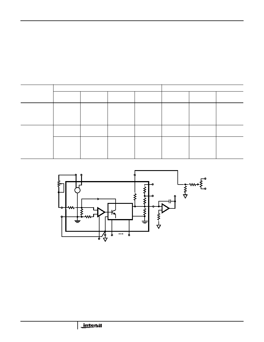
FIGURE 1. UNIPOLAR VOLTAGE OUTPUT
HI-565A
发布紧急采购,3分钟左右您将得到回复。
相关PDF资料
HI1171JCB-T
CONV D/A 8BIT 40MSPS HS 24-SOIC
HI1175JCB-T
CONV A/D 8BIT 20MSPS 24-SOIC
HI1178JCQ
CONV D/A 8BIT TRPL 40MHZ 48-PQFP
HI3-674AKN-5
IC ADC 12BIT 67KSPS 28-SBDIP
HI3-7159A-5Z
IC ADC 5-1/2 DIGIT 28-PDIP
HI3-DAC80V-5
CONV D/A 12BIT OUTPUT AMP 24PDIP
HI3026JCQ
ADC FLASH 8BIT 120MSPS 48-PQFP
HI3338KIBZ
IC DAC 8BIT CMOS 16-SOIC
相关代理商/技术参数
HI1-565AKD-5
制造商:Rochester Electronics LLC 功能描述:24 CDIP, 0+75, +15V,12-BIT D/A CONVERTER W/REF - Bulk 制造商:Harris Corporation 功能描述: 制造商:Intersil Corporation 功能描述:
HI1-565ASD/883
制造商:Intersil Corporation 功能描述:DAC SGL R-2R 12-BIT 24PIN SBDIP - Rail/Tube 制造商:Rochester Electronics LLC 功能描述:DAC 12BIT 6.7MHZ 0.25LSB 24CDIP /883 - Bulk
HI1-565ASD-2
制造商:INTERSIL 制造商全称:Intersil Corporation 功能描述:High Speed, Monolithic D/A Converter with Reference
HI1-565ASD-8
制造商:Rochester Electronics LLC 功能描述:- Bulk
HI1-565ATD/883
制造商:Rochester Electronics LLC 功能描述:24 CDIP, -55+125,+15V,12-BIT D/A CONVERTER W/REF - Bulk 制造商:Harris Corporation 功能描述:
HI1-565ATD-2
功能描述:数模转换器- DAC DAC 12BIT 6 7MHZ 0 1 2LSB 24 S/B DIP MIL
RoHS:否 制造商:Texas Instruments 转换器数量:1 DAC 输出端数量:1 转换速率:2 MSPs 分辨率:16 bit 接口类型:QSPI, SPI, Serial (3-Wire, Microwire) 稳定时间:1 us 最大工作温度:+ 85 C 安装风格:SMD/SMT 封装 / 箱体:SOIC-14 封装:Tube
HI1-565ATD-8
制造商:Rochester Electronics LLC 功能描述:- Bulk 制造商:Harris Corporation 功能描述:
HI1565CDI
制造商:HOLTIC 制造商全称:Holt Integrated Circuits 功能描述:5V Monolithic Dual Transceivers